FPGA Yamanote Line Simulator
A Verilog FSM+datapath simulation of Tokyo's JR Yamanote Line, designed and deployed on a Basys3 FPGA.
This repository contains all the deliverables associated with the design and implementation of a simulator for the JR Yamanote Line in Tokyo running on a Basys3 FPGA. This project was created as a part of the Digital Logic Course (ECE 316) at UT Austin, which I studied abroad in Japan (hence the Tokyo theme) for two months during the Summer 2026 term, which was the first time such an experience was offered.

Design
The Planning Document (linked above) contains the entire design process, including the following steps that were completed before beginning the programming in Verilog:
- Drafting the natural-language specification/proposal laying out the intended operation
- Designing a High-Level State Machine (HLSM) to lay out the state diagram, transition conditions, and the desired logic of each state (such as the panning or next station behavior)
- Decomposing the HLSM into a controller and datapath, deriving 12 control/status signals driven across the datapath/controller boundary to achieve the necessary logic operations and state transitions
- Designing a controller FSM to drive control signals based off the received inputs and status signals received from the datapath
- Designing the entire datapath to actually implement the data operations (using registers, counters, comparators, muxes, etc.) based off the control signals received from the controller
- Laying out the module hierarchy needed to actually implement the project in Verilog. For each module, a port list (with both bitwidths and direction) and list of each instantiated submodule was created.
While each step of this process is present in the aforementioned Planning Document, the natural-language specification and several diagrams of the HLSM, Controller, and Datapath are also provided below for posterity. As with any project, several refinements were made from the original design during the development process — these changes are enumerated at the very end.
Natural-language Specification
The project is a Yamanote Line Simulator, and consists of the following four modes:
OFF (Mode 0): We begin at the default stage with the 7 segment display holding the output “OFF”. The 16 lights at the bottom of the FPGA board are all turned off. You can press BTNU to begin the game and advance to Mode 1.
Station Selection (Mode 1): A starting station, direction, and ending station on the Yamanote Line are chosen. The text “RIDE TO” plus the name of the randomly chosen ending station is looped on the display. Once the user has read it, they can press BTNU to begin playing. Since this is the same button that is used to go from Mode 0 to Mode 1, a rising edge detector is used to ensure that the user cannot just hold down the button and skip this crucial information stage.
The Ride (Mode 2): The display cycles through each train station based on the direction. Each station name pans to the right once, followed by the next station name. This is the main animation for this project, although there are several others in the other modes. We display the names of stops on the Yamanote line in either the clockwise or counter-clockwise direction, depending on the value of the randomly chosen direction bit. The max length of a station name is 16 characters, and most are longer than 5 characters, allowing us to demonstrate non-trivial panning behavior. The 16 lights at the bottom are also set to the station number in binary, simulating riding a train and arriving at progressively higher station numbers. The panning behavior and the transition to each station is done using a slow clock.
Arrival & Exit (Mode 3): To simulate the IC scan off the train, press BTNU one last time. Again, a rising edge detector is used to ensure the user doesn’t just scan instantly by pressing too long when going from Mode 1 to Mode 2.
- If you get off at the correct station: The game ends, prints a win message, and returns to the off state.
- If you get off at the wrong station: The game ends, prints a loss message, and returns to the off state.
System Controls: You can stop at any time by holding the pause switch (SW[0]) high. Once the switch falls low again, the system will resume. The HLSM will remember its current state upon resuming.
Project Architecture
HLSM

Datapath & Controller
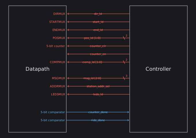


Module hierarchy
ad_sign_top
- controller
  - rising_edge_detector
- datapath
  - clkdiv (×2, width parameterized)
  - lfsr (×3 for dir, start, end, width parameterized)
  - pos_counter
  - clk_counter
  - mag_cmp (×2 for counter_done, ride_done)
  - station_name_rom
  - str_len_rom
  - message_mux
  - window_select
  - ascii_to_7seg (×4, one per each 7 segment)
  - time_mux_sm
Directory structure
.
├── Basys3_Master.xdc
├── README.md
├── rtl
│   ├── ad_sign_top.v
│   ├── ascii_to_7seg.v
│   ├── clk_counter.v
│   ├── clk_div.v
│   ├── controller.v
│   ├── datapath.v
│   ├── message_mux.v
│   ├── pos_counter.v
│   ├── rising_edge_detector.v
│   ├── station_name_rom.v
│   ├── string_len_rom.v
│   ├── time_mux_sm.v
│   └── window_select.v
└── tb
    ├── prompts.md
    ├── tb_ad_sign_top.v
    ├── tb_ascii_to_7seg.v
    ├── tb_controller.v
    └── tb_pos_counter.v
Integration and Simulation
Testbench of Top Level Module
The testbench verifies the following integration scenarios:
- OFF → SELECT: Press BTNU to wake the system from OFF. The sign should display the random target message “RIDE TO <STATION>”
- SELECT → RESET1 → RIDE: Press BTNU again to start the ride loop
- RIDE: Verify that the 7-segment display steps/scrolls through stations while updating the LED pattern to the station number in binary
- Toggling the pause switch freezes
posandclk_counter(visible as a staticssegsequence) - Releasing pause resumes panning from the frozen position — the next position must be the one that would have followed the frozen one, not position 0.
- WIN: Press BTNU exactly when the train reaches the target destination station (
ride_done= 1), verifying the 7 segment display pans “RIGHT STATION”. - LOSE: In a separate test run, press BTNU at the wrong station (
ride_done= 0), verifying the 7 segment display pans “WRONG STATION”. - Return to OFF: Press BTNU on the win/lose screen to return the system to OFF. Also, after the win/loss message scrolls fully, the system should automatically return to OFF on its own.
Simulation Waveform
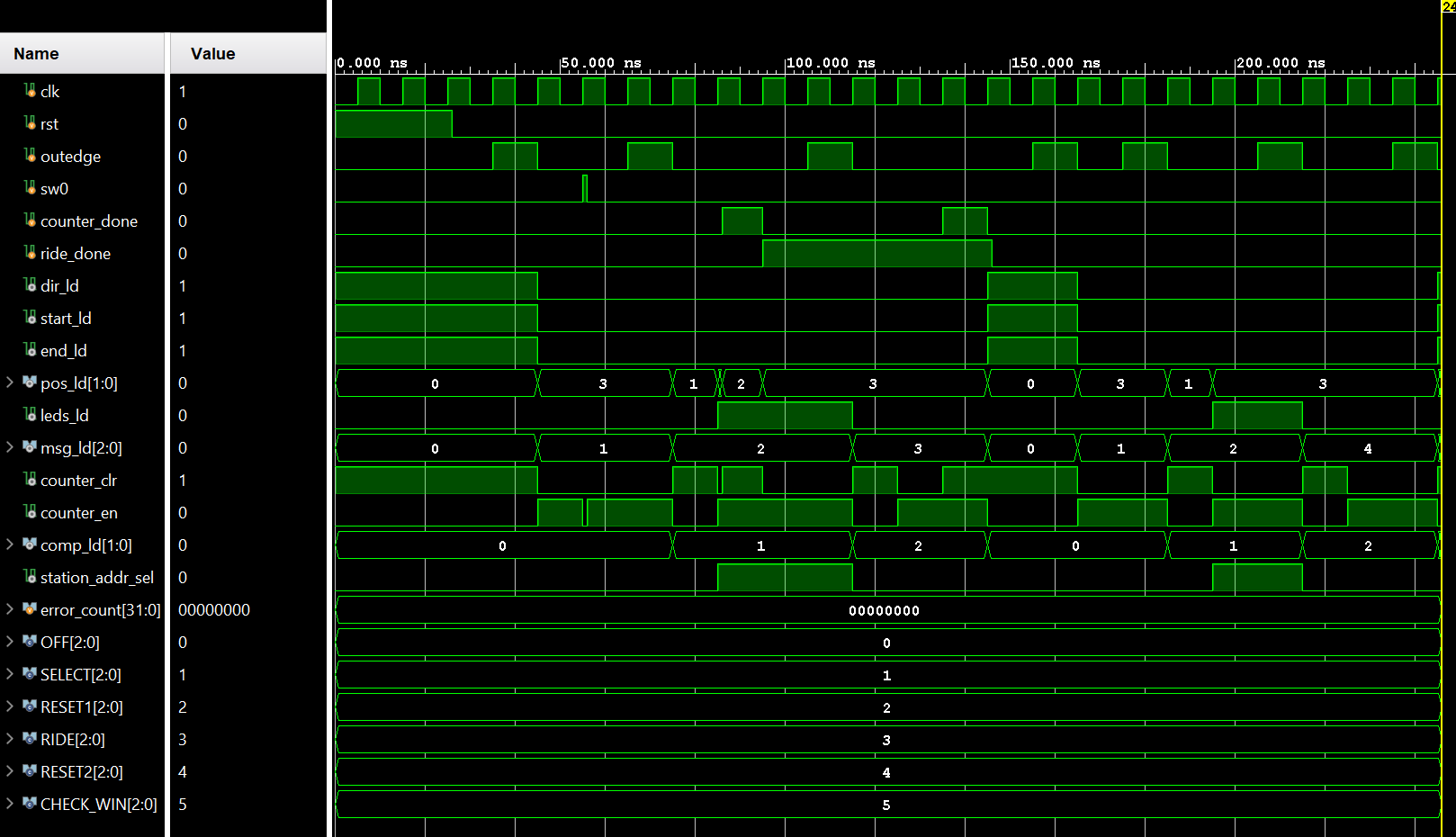
Testbench of Controller FSM
The testbench verifies the following scenarios:
- Cycles through every state (either by pulsing outedge for one clock cycle, or in the case of the last state also testing if the transition occurs when the
counter_donecontrol signal is asserted/the message has looped once) - Checks getting off at both the RIGHT and WRONG station (indicated by
ride_done) to verify a different message is loaded (indicated bymsg_ld)
Simulation Waveform
Other Testbenches
The testbenches for the ascii_to_7seg and pos_counter modules (as well as their associated waveforms) can be found in the tb folder, along with the AI prompts used to generate the testbenches.
Hardware Deployment
Constraints
| Port | Pin | Basys3 Component |
|---|---|---|
| clk | W5 | 100 MHz internal clock |
| BTNU | T18 | Button BTNU (mode advance) |
| sw0 | V17 | Switch SW0 (pause) |
| leds[0] | U16 | LED LD0 |
| leds[1] | E19 | LED LD1 |
| leds[2] | U19 | LED LD2 |
| leds[3] | V19 | LED LD3 |
| leds[4] | W18 | LED LD4 |
| outedge_led | L1 | LED LD15 (rising edge debug LED) |
| an[0] | U2 | Anode AN0 |
| an[1] | U4 | Anode AN1 |
| an[2] | V4 | Anode AN2 |
| an[3] | W4 | Anode AN3 |
| seg[6] | W7 | Segment a (active low) |
| seg[5] | W6 | Segment b (active low) |
| seg[4] | U8 | Segment c (active low) |
| seg[3] | V8 | Segment d (active low) |
| seg[2] | U5 | Segment e (active low) |
| seg[1] | V5 | Segment f (active low) |
| seg[0] | U7 | Segment g (active low) |
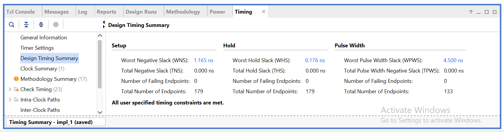
Timing Summary
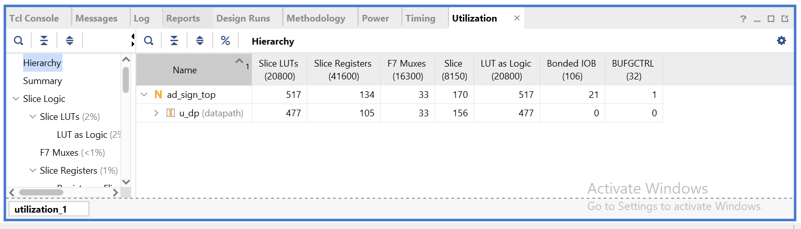
Utilization Summary
Design Changes Made During Implementation
- Instead of having a whole separate magnitude comparator module (
mag_cmp) and instantiating it in the datapath, a logical operator was used instead (as seen in lines likeassign counter_done = (clk_ctr == comp_target)). - The LFSRs were replaced with clock counters for randomness, as the clock cycles so fast that when the user presses at any given moment the current value of the start and end station (as well as direction) appear random. This has the effect of simplifying things, as well as making the testbench deterministic since the value will always be the same after x clock cycles. However, to ensure
start != end, the counters are incremented by different values. - A
rstsignal was added to the port list of many different modules (like the rising_edge_detector FSM) to ensure the initial state would be correct. - The wraparound check was moved to when
poswas actively incremented or decremented to prevent it from being 31 for one clock cycle (even using a modulo wouldn’t work since -1 underflows to 31). - A new
rising_edge_detectorinstance was added toclk_counterso it wouldn’t count for millions of clock cycles every time the slow clock went high. In the same manner, theslow_clkcount was reset at the same time as theclk_counterto prevent the system from being in the middle of aslow_clkcycle during a transition (which would cause the first character to scroll by very fast). - Debouncing was added to the
rising_edge_detectorto prevent multiple state transitions on one button press. - Other minor implementation changes include changing the addresses used to select the current message (collapsing everything into one mux instead of two) and modifying the port list to add
sw0as an input to thecontrollerso that pause functionality could be implemented.